Comparing Nvidia GPU vs AMD GPU vs Google TPU Architectures from a Programmer's Perspective
By Arya Tschand
Introduction
In their Turing Award lecture, Hennessy and Patterson argued that specialization is the primary path forward for performance. Since then, modern machine learning accelerators have made aggressive architectural tradeoffs around parallelism, memory movement, and specialized hardware units where "one size never fits all." Nvidia GPUs, AMD GPUs, and Google TPU have emerged as the most successful ML accelerators by making big bets on very different design decisions.
While they all offer enormous theoretical throughput, achieving even a fraction of peak performance requires programming styles that are tightly coupled to architectural details. Small differences in execution width, memory hierarchy, synchronization, or data movement can lead to order of magnitude performance gaps. As accelerator designs continue to diverge, performance portability becomes less realistic and hardware specific reasoning becomes unavoidable. This blog post focuses on the architectural differences that matter most from a programmer's perspective, and how those differences shape kernel optimization strategies across modern Nvidia GPUs, AMD GPUs, and Google TPUs.

Architectural comparison across Nvidia Blackwell GPU, AMD MI350 GPU, and Google TPU v7 (Ironwood), highlighting key differences in compute architecture, programming model, execution model, memory hierarchy, and system scalability.
My research focuses on hardware-aware kernel optimization. If we want to generate high performance kernels automatically, we need a deep understanding of the hardware and a precise way to communicate those details through context, examples, and profiling feedback. The target programmer in this setting is often an LLM, but the same principles apply to humans. Performance comes from exploiting architectural details rather than writing generic code. Over the past few years, I've had the opportunity to work on LLM-driven kernel optimization research across all three major accelerator ecosystems. I interned at AMD Research last summer working on the MI300 and MI350 GPUs (and published SwizzlePerf in the NeurIPS 2025 ML for Systems Workshop), will be interning at Google Research soon working on the TPUv7, and will also be publishing an academic paper soon where we worked across Nvidia Ampere, Hopper, and Blackwell GPUs. From these experiences and my background as a computer architect, I've spent much of my time learning how to co-design kernels with GPU architectures and how to pass this knowledge along to LLMs to implement hardware-specific optimizations.
In this post, I'll walk through the architectural differences that matter most to programmers across modern Nvidia GPUs, AMD GPUs, and Google TPUs. The goal is not to rank hardware, but to explain how the mental model for programming changes across these systems. I hope this serves both as a resource for programmers learning a new accelerator and as a document that can be dropped directly into the context of the next generation of GPU programming agents!
Nvidia GPUs (Ampere, Hopper, Blackwell)
Nvidia GPUs are likely the most familiar architecture for programmers, but from a kernel optimization perspective they are distinct architectures with meaningfully different constraints. While CUDA provides a stable surface, peak performance depends on explicitly exploiting generation specific hardware features. Kernels that are carefully tuned for one generation often perform poorly on the next, and in some cases rely on instructions or memory paths that no longer exist.
Ampere: Tensor Cores as the Baseline
Ampere is the point where tensor cores become unavoidable for high performance kernels, as earlier generations treated them as an optional fast path but Ampere shifts the balance such that most dense linear algebra workloads must use tensor core instructions to remain competitive. From a programmer's perspective, this shows up primarily through the supported data types and instruction shapes. Ampere expands support for FP16, BF16, TF32, and INT8 tensor core operations, making performance highly sensitive to whether the computation maps cleanly onto these formats. Choosing accumulation type, tile shape, and layout becomes part of kernel design rather than an afterthought, while Ampere's introduction of asynchronous copy instructions from global memory into shared memory fundamentally changes how tiled kernels are written. Rather than a simple load-then-compute structure, performant kernels explicitly stage data through shared memory using software pipelining, requiring the programmer to reason about double buffering, shared memory layout, and instruction ordering to overlap data movement with compute. These changes tighten the relationship between register usage, shared memory consumption, and occupancy, leading many high performance Ampere kernels to operate at low occupancy by design, trading parallelism for data reuse and instruction throughput. Profiling becomes essential in this regime because the limiting factor is often a subtle interaction between resource usage and instruction scheduling.
Hopper: Tensor Memory Accelerator and Explicit Data Movement
Hopper introduces a much more radical shift with the Tensor Memory Accelerator, which allows bulk data movement to be offloaded to dedicated hardware engines instead of issuing asynchronous copies directly from threads. This separates data movement from computation more cleanly than in Ampere, but only if the programmer explicitly opts into the new model. Using TMA fundamentally changes how kernels are structured, as memory transfers are now described at a higher level in terms of multidimensional tiles and launched independently of the compute warps. While this enables deeper software pipelines and better overlap between data movement and computation, it also introduces new failure modes where misaligned tiles or poorly chosen transfer sizes can silently cap performance. Hopper also expands tensor core capabilities with better support for FP8 formats, which significantly affect kernel design as accumulation strategies, numerical stability, and instruction selection must all be reconsidered when porting kernels from Ampere to Hopper. It is important to note that Hopper kernels relying on TMA and specific synchronization primitives do not automatically map well to other architectures, making the programming model more explicit and less portable while requiring automated kernel generation systems to search over memory movement strategies in addition to compute tiling.
Blackwell: TMEM and Programmer Managed On Chip Memory
Blackwell pushes this trend even further by introducing TMEM, a new on-chip memory abstraction that sits alongside registers and shared memory, exposing more direct control over data residency and lifetime while shifting significant responsibility to the programmer. To use TMEM effectively, kernels must be redesigned around explicit memory allocation and reuse patterns, as assumptions that held for shared memory on Ampere or Hopper often no longer apply. Optimal tile sizes, buffering strategies, and synchronization patterns can change dramatically. Blackwell also further expands tensor core instruction variants and low precision support, where structured sparsity and new data formats introduce additional degrees of freedom that only pay off if kernels are written to target them explicitly, meaning code that simply compiles for Blackwell without redesign rarely achieves meaningful speedups. From a programmer's perspective, Blackwell feels less like a new execution model layered on top of CUDA and more like a fundamental shift in how memory and computation are managed. Kernels optimized for Hopper may underperform or fail to compile if they rely on assumptions about memory movement or synchronization that no longer hold, and the many new programmer-exposed hardware changes require kernels to be rewritten around new libraries, syntax, memory lifetimes, tiling strategies, and synchronization patterns rather than lightly adapted from previous generations.
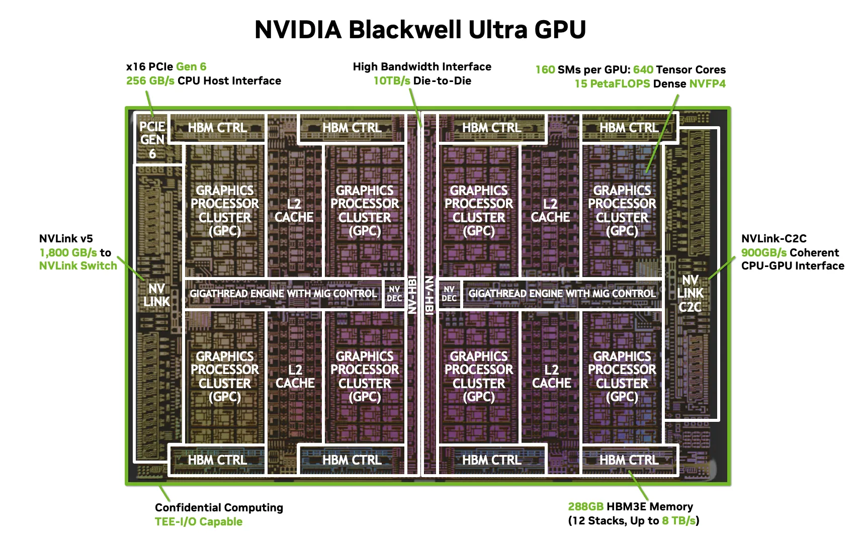
Nvidia Blackwell GPU architecture.
Portability and the Cost of Specialization
These generational shifts explain why high quality kernels take so long to port to new Nvidia architectures. Each generation introduces new hardware units, new memory abstractions, and new preferred execution patterns that require rewriting kernels rather than simply recompiling them. This trend is unlikely to slow down, as future architectures like Rubin are expected to expose even more control over memory allocation and scheduling, which enables higher performance ceilings but also increases the burden on both programmers and automated systems. Performance portability across Nvidia GPUs is already limited, and as specialization deepens, hardware-aware co-design will become even more essential to achieving competitive performance.
AMD GPU (MI300, MI350)
AMD GPUs share many surface level similarities with Nvidia GPUs, including explicit control over memory and synchronization. However, MI300 and MI350 use a SIMD execution model rather than SIMT, and differ enough that naive ports of well tuned CUDA kernels often perform poorly. These differences show up in execution width, instruction exposure, memory behavior, and device topology, all of which directly affect how kernels must be written and optimized.
Execution Model, Instructions, and Memory Behavior
AMD GPUs execute threads in 64-thread wavefronts using a SIMD execution model, which fundamentally changes the cost model for divergence compared to Nvidia's 32-thread SIMT warps. Control flow that is only mildly inefficient on Nvidia hardware can serialize a much larger fraction of execution on AMD GPUs, meaning branch-heavy kernels often need to be rewritten using predication or data parallel formulations. Vectorization and instruction packing become more central concerns in this model, and kernels that assume narrow execution groups tend to underutilize the available hardware resources. MI300 and MI350 include 4th generation Matrix Cores for throughput-oriented vector and matrix execution, but they are exposed through a lower level programming model than Nvidia tensor cores, making performance highly sensitive to instruction shapes, data layout, and alignment. Kernels designed around Nvidia tensor core assumptions often do not map cleanly onto AMD hardware without substantial restructuring, and in contrast to Nvidia where tensor core usage is frequently implicit, AMD often requires more explicit control from the programmer to reach peak performance. The memory hierarchy further complicates portability, as the combination of LDS (Local Data Share), L2 cache, and Infinity Cache behaves quite differently than Nvidia's shared memory and cache hierarchy, significantly affecting tiling strategies and kernel structure in ways that make profiling essential to understand whether performance is limited by memory bandwidth, synchronization overhead, or instruction throughput.
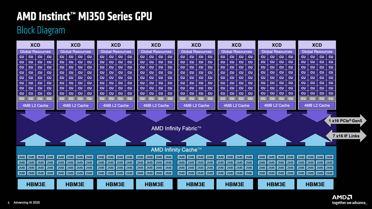
AMD MI350 GPU architecture.
Chiplets, Locality, and Hardware Aware Co Design
MI300 and MI350 are built from eight Accelerator Compute Dies (XCDs) plus two I/O dies connected through a bidirectional interconnect using Infinity Fabric, and while the memory space appears unified, physical locality matters significantly as the cost of accessing data depends on where it resides relative to the executing wavefront. Default scheduling does not guarantee locality-aware execution. For kernels that span the full device, data placement and grid decomposition can dominate performance, and two kernels with identical instruction counts can behave very differently depending on how much traffic crosses XCD boundaries, with these effects often invisible at the source level and only becoming apparent through careful profiling. In SwizzlePerf, we show that explicitly exposing XCD layout and default scheduling behavior to an LLM enables it to generate kernels that significantly outperform naive implementations by remapping thread blocks to better align work with XCD-local memory, thereby reducing cross-chiplet communication and achieving substantial speedups. This demonstrates that AMD GPUs strongly reward hardware-aware co-design for both human programmers and automated systems, and overall, MI300 and MI350 should be treated as distinct architectural targets rather than drop-in replacements for Nvidia GPUs, as differences in execution width (64-thread wavefronts vs 32-thread warps), instruction exposure, memory behavior, and multi-chiplet topology all fundamentally shape how high performance kernels must be written.
Google TPU (v7 Ironwood)
Google TPUs differ from GPUs not just in microarchitecture, but in how much of the execution model is fixed ahead of time. GPUs are designed to tolerate irregularity through massive multithreading and dynamic scheduling. TPUs instead assume regular structure and reward programs that make data movement and computation explicit at compile time. This difference fundamentally changes how kernels are written and optimized.
Systolic Arrays, Pallas, and Explicit Dataflow
At the core of a TPU is a large systolic array optimized for dense matrix operations. TPUv7 Ironwood uses 256×256 systolic arrays arranged in a 3D torus topology for dedicated tensor math, where the array expects data to arrive in a precise order and at a precise cadence. Unlike GPUs where threads dynamically fetch data as needed, TPUs rely on deterministic systolic dataflow using VLIW instructions that operate without instruction fetch overhead during matrix cycles, and Pallas exposes this model directly to the programmer in a way that feels fundamentally different from GPU programming. Rather than writing kernels in terms of threads and blocks, you describe tiled computations and explicitly specify how data is loaded, stored, and reused through static software-directed DMA scheduled by the XLA compiler, with control flow deliberately restricted and irregular memory access patterns strongly discouraged. To achieve good performance, problems often need to be reshaped to match the systolic array dimensions and dataflow constraints, making TPU programming feel less like writing a kernel and more like designing a dataflow graph where loop structure, tile sizes, and memory layout decisions are central to success. Performance ultimately comes from keeping the systolic array fully utilized and minimizing stalls caused by poorly planned data movement, a constraint that shapes every aspect of how TPU kernels are designed.
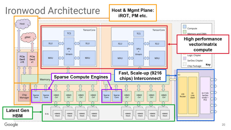
Google TPU v7 (Ironwood) architecture.
Compilation, Global Scheduling, and TPU v7
TPU performance is driven by ahead-of-time compilation rather than dynamic scheduling, with the XLA compiler performing aggressive global analysis to determine how computation, memory transfers, and collectives are interleaved across the entire program. Unlike GPUs where individual kernels can often be tuned in isolation, TPU performance depends critically on how all pieces fit together as a unified whole. TPU v7 pushes this model further by increasing compute density and bandwidth while also expanding the scale at which communication matters, with Optical Circuit Switching (OCS) enabling dynamic reconfiguration of pods up to 9,216 chips with 96 Tb/s ICI, which means the cost of poor sharding or suboptimal tiling increases substantially as more of the system operates in lockstep. Decisions about tile shapes, data partitioning, and collective placement become even more important than in earlier generations, and for Pallas programmers this means kernels often need to be rewritten to align with the 256×256 systolic array dimensions, memory capacities (32MiB VMEM, 128MiB CMEM, 192GB HBM3e), and communication patterns introduced in v7. Code that worked well on earlier TPUs may compile but fail to reach expected performance if it does not fully utilize the updated systolic array or introduces unnecessary synchronization points, and the high locality sensitivity of the 3D torus mesh requires precise data placement to avoid expensive non-local memory accesses that can severely degrade overall throughput.
Implications for Kernel Generation and Optimization
For autonomous kernel optimization, TPUs present a different challenge than GPUs. The constrained execution model reduces the space of valid programs which can make search easier, but at the same time, global decisions dominate performance such that a single poor choice in tiling, sharding, or memory layout can degrade performance across the entire program. Effective optimization therefore requires a deep understanding of how high-level operations map onto the systolic array and how communication patterns interact with the TPU topology, making hardware awareness not just beneficial but essential. On TPUs, hardware awareness is the fundamental difference between a program that simply runs and one that actually performs well enough to justify the specialized hardware.
Closing Thoughts
As ML accelerators continue to specialize, the hardware itself increasingly defines what high performance code looks like. Across Nvidia GPUs, AMD GPUs, and Google TPUs, the dominant performance factors are no longer hidden behind abstractions. Execution width, memory movement, locality, and scheduling are all programmer visible, and getting them wrong can lead to order of magnitude slowdowns. This makes hardware awareness a first class requirement rather than an optional optimization.
These trends are especially important for LLM driven kernel optimization. If we expect LLMs to generate or adapt high performance kernels, they must be grounded in accurate architectural models and guided by profiling feedback that reflects real hardware constraints. Generic reasoning or portability assumptions are insufficient when kernels must be co designed with tensor cores, chiplets, or systolic arrays in mind. As architectures continue to diverge and expose more explicit control, the success of automated kernel generation will depend on how well we encode and communicate hardware specific knowledge.
Thanks for reading - feel free to reach out to me via email (aryatschand@g.harvard.edu) or X (@AryaTschand) with any questions, feedback, or suggested changes/fixes!